Ever wonder how the complex electronics in your phone, laptop, or even your home’s solar inverter are made so small and powerful? The magic happens through a highly precise manufacturing method. If you’ve ever asked, what is the surface mount technology process?, you’re in the right place.
Table of Contents
At RenewGenius, we believe in making complex technology understandable, whether it’s how solar panels generate power or how the electronics that manage them are built. This article, and our accompanying surface mount technology video, will break down the core manufacturing method behind most modern electronics.
Let’s get the SMT process explained in five simple, easy-to-understand steps.
Before We Begin: What is Surface Mount Technology (SMT)?
Surface Mount Technology, or SMT, is a method for producing electronic circuits by mounting components directly onto the surface of a printed circuit board (PCB). This is a major evolution from the older through-hole method, where component leads were inserted through holes in the board and soldered on the other side.
SMT is what allows for the incredible miniaturization and efficiency we see in today’s devices, from compact solar monitoring systems to smartphones.
The SMT Process Explained in 5 Steps
The entire SMT assembly line is a marvel of automation and precision. Here’s how a bare board becomes a fully functional electronic brain.
Step 1: Solder Paste Printing
The first step is to apply a foundation for the components. A machine applies a sticky, metallic solder paste to the circuit board. This isn’t just a simple coating; a stencil is laid over the board, ensuring the paste is applied only to the specific pads where components will be soldered. Think of it like screen-printing a t-shirt, but with metallic paste and on a much smaller, more precise scale.

Step 2: Component Placement (Pick-and-Place)
This is where the high-speed action happens. An automated “pick-and-place” machine, loaded with reels of tiny electronic components (like resistors, capacitors, and ICs), picks up each component and places it exactly where it belongs on the board, right onto the waiting solder paste. These machines work at incredible speeds, placing thousands of components per hour with pinpoint accuracy that would be impossible for a human hand.
Step 3: Reflow Soldering
With all the components sitting on the solder paste, the boards are sent through a long reflow oven. The oven uses a carefully controlled temperature profile to heat the boards, which accomplishes two main things:
- It activates the “flux” in the paste to clean the surfaces for soldering.
- It melts the solder, creating strong, permanent electrical connections for every component.
The board is then cooled in a controlled manner to solidify the solder joints.
Step 4: Inspection (AOI)
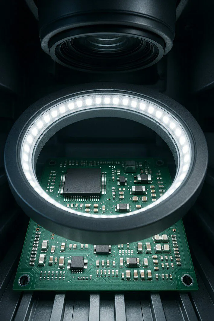
Quality control is critical. After the reflow process, the boards are inspected to ensure every component is correctly placed and soldered. This is often done using an Automated Optical Inspection (AOI) machine. The AOI machine uses cameras to scan the board and compare it to a perfect reference image, flagging any potential defects like missing components, incorrect placement, or poor solder joints.

Step 5: Cleaning and Testing
Finally, the completed boards may be washed to remove any flux residue, which could cause issues over time. The last and most important part of the PCBA process is a functional test. The board is powered up and tested to ensure it works exactly as designed, ready to be installed into its final product.
Why Understanding the SMT Process Matters
Understanding how technology is made helps you appreciate its value. At RenewGenius, our comprehensive solar knowledge base is designed to empower homeowners with this kind of clarity. Just as an efficient SMT process leads to reliable and cost-effective electronics for residential solar solutions, understanding your solar options helps you make a confident investment. An efficient process, whether in manufacturing or in calculating your energy savings with our ROI calculator, is key to achieving the best outcome.
SMT vs. THT: A Key Part of the PCBA Process
SMT is the dominant method for modern electronics, but it’s not the only one. It’s one part of the wider PCBA process. For components that need to withstand more mechanical stress, manufacturers might use the older Through-Hole Technology (THT). Each has its place, and understanding the differences is key for product designers. To learn more about the complete assembly workflow and a direct comparison of Surface-Mount Technology (SMT) versus Through-Hole Technology (THT) https://pcbapros.com/services/pcba-manufacturing/, our detailed guide provides a deeper dive.
From Tiny Circuits to Big Savings
From solder paste to a final, functional board, the SMT process is a five-step journey of precision and automation. It’s this incredible technology that powers the devices we rely on every day.
If you’re ready to put modern technology to work for your home with a solar energy system, contact RenewGenius. We make the process of going solar just as simple and clear.

